Z-AXIS provides electronic design and electronic contract manufacturing services. Welcome to our three-part video series electronic circuit design.
Electronic Design: Part 1
This video is the first in a three-part series, and it describes our electronic design process from the requirements document through the design review.
Requirements Document and Statement of Work
Some companies come to us with a detailed requirements document and a statement of work. Others know what they want a product to do but aren’t sure how to get there. Either way, our design engineers can help.
Based on your requirements, Z-AXIS will provide a proposal with a timeline, milestones, and costs. The first phase could be a feasibility study, and many projects need a basic prototype. The key is to de-risk your project.
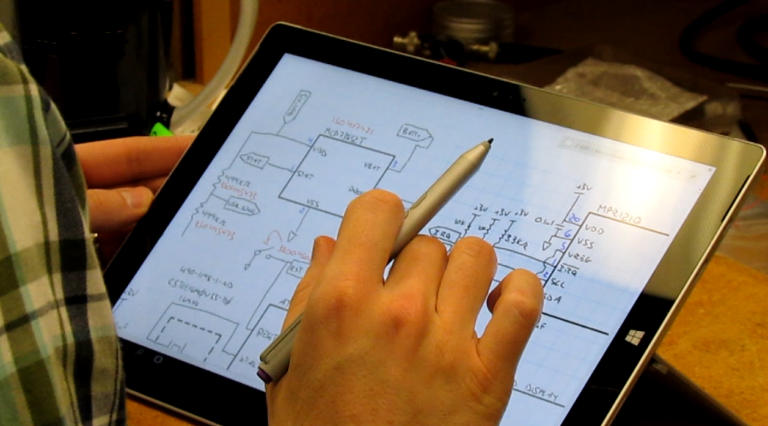
Design Work and Block Diagram
Next, detailed design work begins with a block diagram. Each block represents a function, such as battery protection circuitry. We’ll then create the circuits for each block and find the best solution.
This might surprise you, but it takes more time to source parts that to design circuits. There are specifications to compare and issues such as pricing, availability, and sourcing to consider.
By making smarter choices during the design process, you can avoid production delays later on. That’s why even if you’ve identified all of the components that you need, Z-AXIS may suggest some alternatives.
Schematic Capture and SPICE
Although we use parts from our design library whenever possible, we can also define and add new parts as necessary. Then, once your preliminary design is complete, it’s time for schematic capture.
Using CAD software called PADS, our technicians draw your actual circuit diagram. Then they simulate your electrical circuit using software called SPICE.
When SPICE is complete, it’s time for the design review. That’s when a team of design engineers looks for flaws and ensures that all of your requirements are met. Two heads are better than one, and a team of engineers is best of all.
In our next Electronic Design series video, you’ll see how Z-AXIS performs a printed circuit board layout. In the meantime, let us know what you need.
Electronic Design: Part 2
This video is the second in a three-part series, and it describes what happens after the design review is complete.
Physical Layout and Schematic
After the design review process is complete, the physical layout of your board begins. A board designer creates an outline that fits the available space and imports your schematic, a drawing that defines connections between components.
When your schematic is imported, however, all of the parts are in a pile that we call a rat’s nest. A technician then drags individual components into position. The lines, or connections, between parts are known as rubber bands. As the parts move, the rubber bands move as well.
When moving the parts, the technician needs to keep some important things in mind. For example, high voltages need large spaces, and large currents need large trace widths. Concerns about noise and EMI need to be addressed as well. Usually, there are also some mechanical concerns, such as the positions of switches or connectors.
DFM, Gerber File, and Board Array
Still, there are some things you can’t tell from a schematic. That’s why the board designer works closely with the lead electrical engineer, and your design is reviewed at multiple levels. During the layout review, a manufacturing engineer looks at design for manufacturability (DFM), such as how to make sure there’s enough room to hold your board during production.
Next, we create a Gerber file that captures all of the layers of your board. This industry-standard file format includes the copper layers, holes, solder mask, silk screen, and board outline.
Using CAM 350, we then create an array of boards that are sized for our manufacturing equipment. This array supports the cost-effective use of a PCB substrate panel and it creates fiducials for our pick-and-place machines.
Bare Boards and a Stainless Steel Stencil
Next, we order bare boards for your project. Generally, it takes a few days to several weeks until they arrive for inspection. We also export the BOM, or bill of materials, from the schematic to order all of your parts, typically from distributors.
CAM 350 also enables us to order a stencil that’s laser cut from stainless steel. This stencil contains holes so that we can apply solder paste to the metal areas of your board. Z-AXIS has a considerable amount of experience in this area and uses a high yield process.
In our next video, the final one in our three-part series, you’ll see how our mechanical design process supports electronic design.
Electronic Design (Part 3)
Coming Soon!