By following these design recommendations, you can reduce the cost of your boards and ensure their manufacturability.
Z-AXIS provides electronic design and manufacturing services all under one roof. Whether we design your printed circuit boards (PCB) from scratch or work from your existing plans, our design for manufacturing (DFM) assistance can save you time and money. In this white paper, we examine the 10 most common mistakes that we see during PCB design. We also explain how to avoid them.
By following the design recommendations in this document, you can reduce the cost of your boards and ensure their manufacturability. Boards that are easier to make are faster and less expensive to produce. Plus, PCB designs that are free from flaws support higher levels of quality and performance. Each design is different, of course, but the information in this white paper applies to your project.
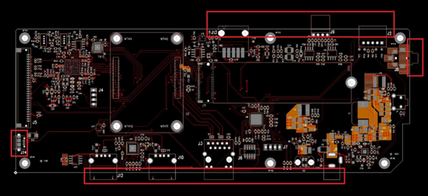
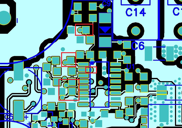
Figure 1: The red boxes show how connectors extend from all four edges of the board.
1. Don’t Place Parts Too Close to the Edge of the Board
Sometimes, the bare boards that an electronic contract manufacturer (ECM) receives are slightly smaller than what the ECM ordered. If your PCB design puts a pad too close to the edge, there’s a risk of nicking the side of the pad during assembly. Parts can overhang the edge of the board, but good designs keep the pads inside the board’s footprint.
The standard tolerance for the length and width of a PCB is ± .020 inches. If your board uses surface mount technology (SMT) to attach components, leave some additional room so your ECM can hold the board in place throughout the SMT process. Otherwise, your manufacturer will need to use rails or fixtures to hold the PCB – and that will increase your manufacturing costs.
Z-AXIS recommends following industry-standard tolerances and leaving an additional 0.25 inches on two parallel edges so that we can hold your board without rails or fixtures. It’s also worth noting that odd-shaped boards (like in Figure 1 above) add costs because they require fixtures for handling.
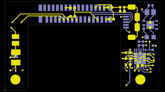
Figure 2: This is an example of a six-layer board that could have used four layers instead.
2. Don’t use more layers than are necessary.
Many of the board layouts that we receive at Z-AXIS use more layers than are necessary. For example, most of the eight-layer boards we see could use six layers, and many of the four-layer boards we see could use just two layers instead. It’s easier for a designer to add more layers than it is to reduce complexity; however, more layers increase the cost of your bare boards. Don’t use more layers than are necessary and ask your ECM for advice if you’re unsure.
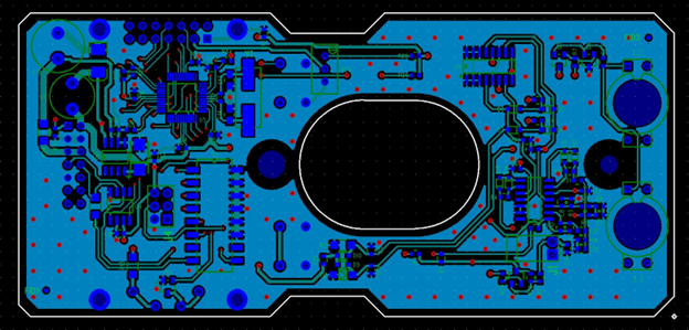
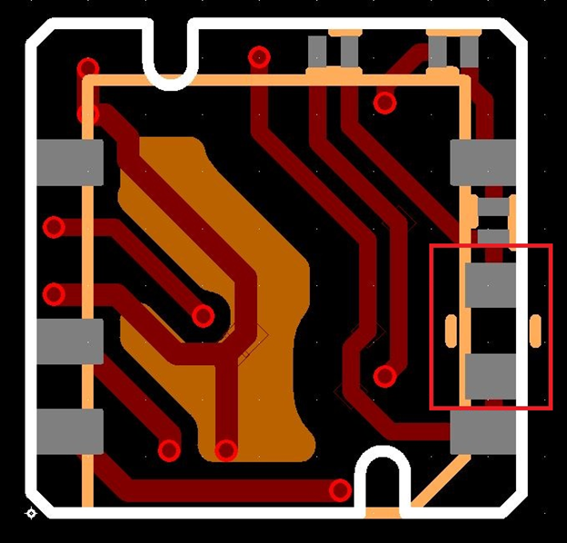
Figure 3: As shown in blue (above), most of the components are on one side of the board. As shown in brown (below), the only SMT components on the board’s opposite side are D1 and D2 (red boxes).
3. Don’t put parts on both sides of a board if you can avoid it.
Two-sided boards are more expensive. Yet some PCB designs put most parts on one side of the board and just a few parts on the other, as shown in Figure 3 above. Let’s say your board includes a large integrated circuit (IC) and your designer wants to put the coupling caps close by. Placing the caps on the other side of the board is convenient for the designer, but it increases your manufacturing costs since the board must be flipped over during production.
Think of all of the steps that are involved. At Z-AXIS, we apply solder paste, add parts, send the printed circuit board assembly (PCBA) through a heat tunnel, and then inspect the PCBA. If we need to add components to the other side of the board, we flip the board over and repeat all of these steps. That’s why, whenever possible, we recommend putting all of the parts on the same side of the PCB.
Figure 4: The red arrow shows how there isn’t a solder mask dam between the resistor pad and the switch pad. Consequently, the resistor can float away from its pad.
4. Don’t put SMT pads too close together.
SMT components use solder masks that are larger than their pads. Yet individual solder masks shouldn’t intersect with each other. Otherwise, parts may float toward the center (and each other) during solder reflow. You don’t want one big chunk of copper, and you don’t want parts to move to the middle and hit each other, dislodging components and causing manufacturing defects. To avoid these problems, leave enough room between SMT pads.
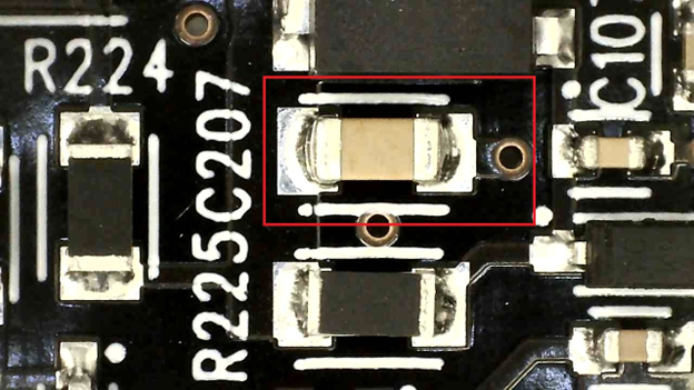
Figure 5: The red boxes show where round vias intersect square SMT pads.
5. Don’t intersect an SMT pad with the solder mask opening for a via.
Vias are copper-plated holes that allow a designer to run a trace from one side of the board to the other. When the trace exits the other side of the board, it runs to the pad for an SMT part. If you intersect an SMT pad with the solder mask opening for the via, solder paste will flow down the via and starve the SMT part’s solder joint. An ECM could use a soldering iron, but that adds costs to your project.
Figure 6: The red box shows a component that is underneath the transformer and extends beyond the edge of the board.
6. Don’t put parts too close together.
During PCB assembly, you don’t want pick-and-place equipment to hit and damage or dislodge nearby parts. Consider, too, that part placement is never perfect. Rather, it just needs to be within tolerance. That’s why it’s important to leave enough room so that the pick-and-place machine won’t cause collisions that can result in lower yields and higher costs.
Figure 7: The red boxes show through-hole components on the top side of the board that have components near pins on the bottom side of the board (not shown). This arrangement complicates soldering.
7. Don’t leave too little room for selective soldering.
Some PCB designs place SMT parts on opposite sides of the board from through-hole technology (THT) parts, and some ECMs use a selective soldering process. To account for mixed board technology, your ECM needs enough room for the selective soldering nozzles to reach the THT parts. Otherwise, soldering the THT parts could wash off the solder from the SMT parts and cause manufacturing defects. At Z-AXIS, we recommend leaving enough room for selective soldering.
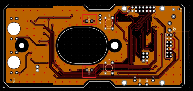
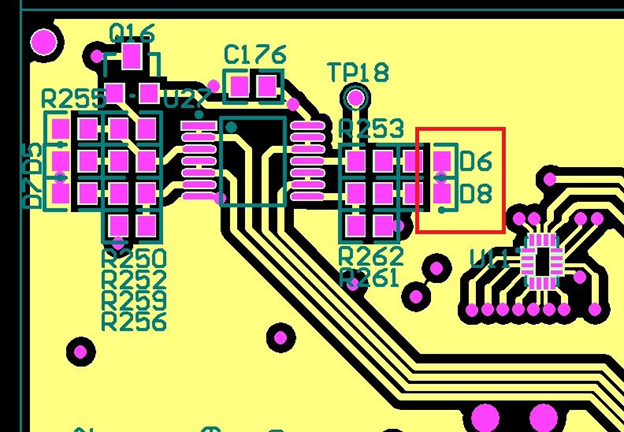
Figure 8: D6 and D8 on the right side (red box) are connected to a large copper flood, but the pads on the left have only a small trace that’s connected to them.
8. Don’t use copper traces with significantly different weights.
Z-AXIS sees board layouts where one of two terminal SMT components is connected to a large ground plane and the other side of the board is connected to a very thin trace. During reflow, the solder that’s used with the lower copper weight melts more easily. In turn, the surface tension causes the part to flip up in a process called tombstoning. That’s why it’s important to balance the weight of the copper that connects to parts like 0402s and 0603s.
Figure 9: The pads do not extend underneath the part.
9. Be careful when creating your own component footprints.
There are many standard SMT component footprints, but some designers create their own. If your pads are too large, however, misalignment may occur. For the best results, check the component footprints that part manufacturers suggest. They’re usually correct, especially with standard parts like 8085s. It’s easy for a busy designer to make mistakes, so use caution when creating custom component footprints.
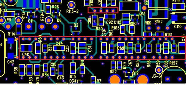
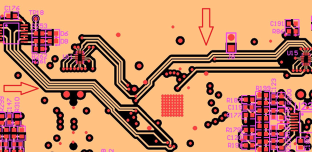
Figure 10: The red arrows show traces running parallel to each other for long distances at a minimum set design rule.
10: Don’t design the entire board to the limit of PCB design rules.
Finally, remember that building a board is an exercise in probability. If you push the envelope unnecessarily, you’ll increase risks and add expenses. By following all of the design recommendations in this white paper, you can get better boards that are easier to manufacture and less expensive to assemble. When it’s time for your next electronics design or manufacturing project, contact Z-AXIS.
Z-AXIS, Inc. 1916 NY-96 Phelps, NY 14532 (315) 548-5000 sales@zaxis.net
Keep up with our latest news.
From contract manufacturing to business news, get the insights you need to advance your business.